POWER GaN HEMT
at the acme Research Group
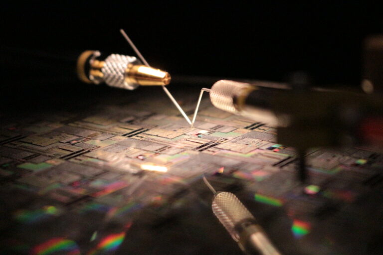
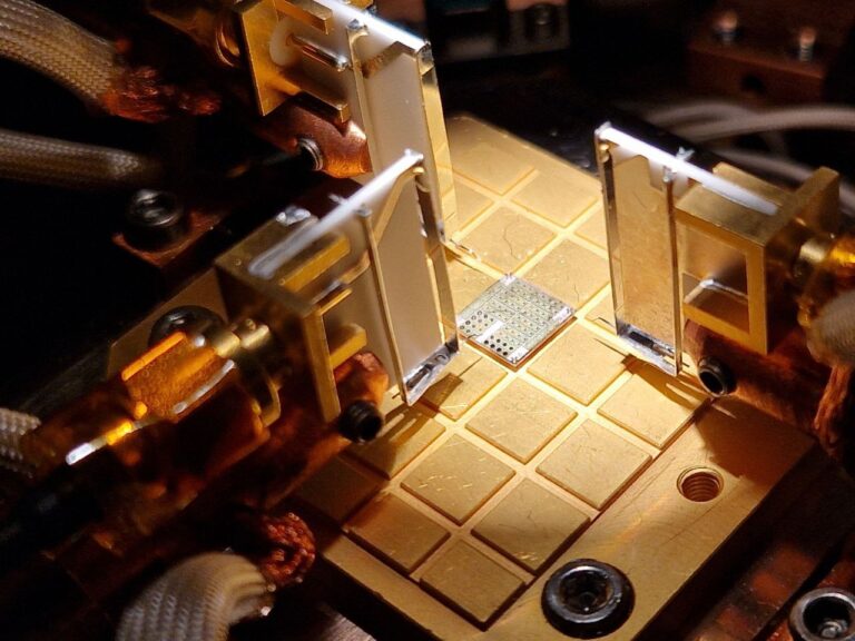
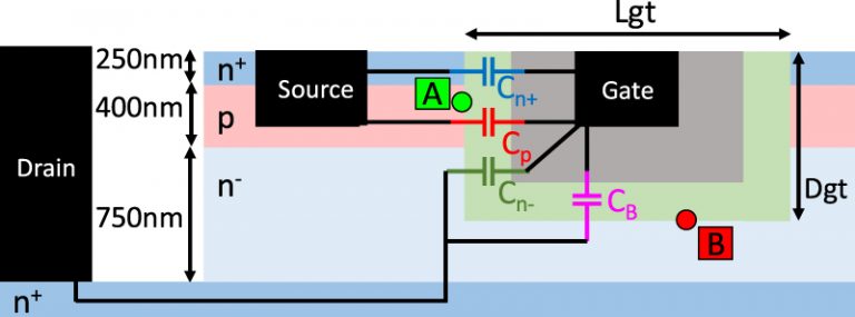
Characterization of GaN based transistors for power applications, and of high-voltage/high current SiC devices.
Analysis of the trapping processes that limit the dynamic performance of the devices, based on current-DLTS, capacitance-DLTS, optical-DLTS, backgating investigation; development of physical models of the charge-trapping processes; study of the interface traps by C-V, Dit and Vth transient measurements; analysis of issues related to devices with Schottky, insulated and p-type gate.
Study of the lifetime-limiting mechanisms in GaN- and SiC-based transistors and diodes; time-dependent dielectric breakdown, instability of the p-type and insulator layers, hot electron effects (studied by electroluminescence) and failure analysis.


